Xiamen Zopin New Material Limited Established in 2011, it is a new material industry with capabilities of independent research & development, production and sales as one. Our ISO9001:2012 factory covers an area of 6 hectares and a building area of 28,000 square meters, with annual production of high-performance metal foams of 250,000 square meters. Our R&D team is composed of academicians and experts from Tsinghua University, Polytechnic University of Hong Kong, Nanyang Technological University, and other domestic and foreign metal foam professionals. After many years’ endeavor, we now own our proprietary intellectual property rights in manufacturing high purity and high porosity metal foams.
Silicon Wafers: Overview, Properties, Fabrication, Applications, and Advantages
Overview
Silicon wafers are the foundational material of the modern semiconductor industry, forming the substrate for integrated circuits, solar cells, and microelectromechanical systems (MEMS). These thin slices of highly pure silicon serve as a platform on which microelectronic devices are fabricated. Silicon’s exceptional electronic properties, abundance, and processability have made it the dominant material for semiconductor manufacturing. Over the past few decades, advancements in silicon wafer production and processing have significantly enhanced the performance, reliability, and scalability of electronic devices, driving the rapid development of technology and renewable energy systems.
Properties
The unique properties of silicon wafers make them ideal for a wide range of electronic and optoelectronic applications:
1. High Purity: Commercial silicon wafers typically contain purity levels above 99.9999% (6N) to minimize defects that can adversely affect device performance.
2. Crystalline Structure: Silicon wafers are available in monocrystalline and polycrystalline forms. Monocrystalline wafers offer uniform electronic properties, while polycrystalline wafers are cost-effective for large-scale applications like photovoltaics.
3. Electrical Characteristics: Silicon is a semiconductor with a bandgap of 1.12 eV at room temperature, enabling controlled conductivity through doping.
4. Thermal Stability: Silicon can withstand high-temperature processing, up to around 1400°C in inert atmospheres, making it suitable for various thermal fabrication steps.
5. Mechanical Strength: Despite their thinness, silicon wafers have sufficient mechanical strength to withstand handling, cutting, and processing during device fabrication.
Fabrication
The fabrication of silicon wafers is a precise and multi-step process designed to achieve uniformity, flatness, and defect-free surfaces:
1. Purification: Silicon is refined from metallurgical-grade silicon into electronic-grade polysilicon through chemical vapor deposition and other purification methods.
2. Crystal Growth: Monocrystalline silicon wafers are produced using the Czochralski (CZ) method or float-zone (FZ) technique. These methods grow large, defect-free single crystals with controlled orientation.
3. Ingot Slicing: Silicon ingots are sliced into thin wafers using diamond wire saws or slurry-based cutting tools. Thickness uniformity is critical to ensure consistent device fabrication.
4. Surface Treatment: Wafers undergo lapping, grinding, and chemical-mechanical polishing (CMP) to achieve a smooth, defect-free surface. This step is essential for subsequent photolithography processes.
5. Doping and Coating (Optional): Wafers may be doped with elements such as boron or phosphorus to achieve desired electronic properties or coated with insulating or conductive layers for specific applications.
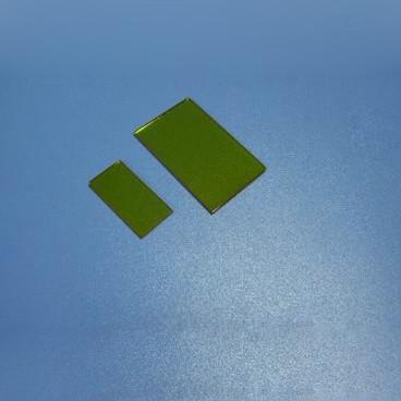
Bismuth silicate Crystal Substrate
Applications
Silicon wafers serve as the backbone for multiple high-tech industries:
1. Semiconductor Devices: Integrated circuits and microchips rely on silicon wafers as substrates for transistor fabrication, forming the core of computers, smartphones, and other electronic devices.
2. Solar Photovoltaics: Silicon wafers are widely used in solar cells, converting sunlight into electricity with high efficiency. Monocrystalline wafers offer superior performance, while polycrystalline wafers reduce production costs.
3. MEMS Devices: Microelectromechanical systems, including sensors, actuators, and microfluidic devices, are built on silicon wafers due to their mechanical precision and compatibility with microfabrication techniques.
4. LED and Optoelectronics: Silicon wafers serve as substrates for certain LED devices, photodetectors, and other optoelectronic components.
5. Research and Development: Silicon wafers are extensively used in materials research, nanotechnology, and experimental electronic devices due to their predictable behavior and standardization.
Advantages
Silicon wafers offer several key advantages that reinforce their central role in technology:
1. Uniformity and Reliability: High-quality wafers provide a consistent platform for microfabrication, ensuring predictable device performance.
2. Scalability: Silicon wafer manufacturing is highly scalable, enabling mass production of electronic components and solar cells.
3. Versatility: Compatible with a wide range of doping, coating, and etching processes, silicon wafers can support diverse applications across electronics, energy, and MEMS.
4. Cost-Effectiveness: While advanced wafers can be expensive, the maturity of silicon processing technology has reduced costs, making silicon devices economically viable for large-scale applications.
Conclusion
Silicon wafers remain an indispensable material in modern technology, underpinning the electronics, renewable energy, and MEMS industries. Their combination of high purity, crystalline uniformity, thermal and mechanical stability, and compatibility with advanced fabrication techniques makes them uniquely suited for complex device manufacturing. Continued innovation in wafer production, surface engineering, and doping strategies promises to enhance performance further, sustaining silicon’s dominance in cutting-edge technology. As both research and industrial applications expand, silicon wafers will continue to serve as the foundation of next-generation electronics and energy solutions.
 Daisy@foam-material.com