Xiamen Zopin New Material Limited Established in 2011, it is a new material industry with capabilities of independent research & development, production and sales as one. Our ISO9001:2012 factory covers an area of 6 hectares and a building area of 28,000 square meters, with annual production of high-performance metal foams of 250,000 square meters. Our R&D team is composed of academicians and experts from Tsinghua University, Polytechnic University of Hong Kong, Nanyang Technological University, and other domestic and foreign metal foam professionals. After many years’ endeavor, we now own our proprietary intellectual property rights in manufacturing high purity and high porosity metal foams.
Wafer Silicon: The Foundation Material for Modern Semiconductor Manufacturing
Introduction
Wafer silicon is the fundamental substrate material used in the fabrication of semiconductor devices, integrated circuits (ICs), microelectromechanical systems (MEMS), power electronics, photovoltaic cells, and various advanced electronic components. As the demand for smaller, faster, and more energyefficient devices continues to grow, highquality wafer silicon has become increasingly critical in supporting innovations across industries such as consumer electronics, automotive, telecommunications, artificial intelligence, and renewable energy.
Manufactured through highly controlled crystal growth and precision processing techniques, wafer silicon provides the ideal platform for building complex microelectronic structures with exceptional electrical, mechanical, and thermal properties. Today, wafer silicon serves as the backbone of the global semiconductor industry and remains indispensable for both research laboratories and largescale industrial production.
What Is Wafer Silicon?
Wafer silicon refers to thin, circular slices of ultrahighpurity crystalline silicon that act as the base substrate for semiconductor device fabrication. These wafers are produced from singlecrystal silicon ingots grown using advanced crystal growth methods such as the Czochralski (CZ) process or the Float Zone (FZ) process.
After crystal growth, the silicon ingot undergoes multiple precision manufacturing steps, including slicing, edge profiling, lapping, etching, polishing, cleaning, and quality inspection, resulting in wafers with mirrorlike surfaces and extremely tight dimensional tolerances.
Wafer silicon is available in various diameters, including:
100 mm (4 inches)
150 mm (6 inches)
200 mm (8 inches)
300 mm (12 inches)
Among these, 300 mm wafer silicon has become the industry standard for advanced semiconductor manufacturing due to its higher production efficiency and lower cost per chip.
Key Characteristics of Wafer Silicon
Highquality wafer silicon possesses several unique properties that make it ideal for precision electronic manufacturing.
UltraHigh Purity
Semiconductorgrade silicon typically achieves purity levels of 99.9999999% (9N) or higher. Extremely low impurity concentrations ensure excellent electrical performance and device reliability.
Excellent Crystal Structure
Singlecrystal wafer silicon provides a highly ordered atomic lattice with minimal crystal defects, enabling consistent electrical characteristics across the entire wafer surface.
Outstanding Surface Flatness
Modern polishing technologies produce mirrorfinished surfaces with nanometerscale roughness, supporting advanced photolithography and thinfilm deposition processes.
Superior Thermal Stability
Silicon maintains excellent mechanical strength and dimensional stability under elevated processing temperatures, making it suitable for hightemperature diffusion, oxidation, and annealing.
Excellent Electrical Properties
Through precise doping with elements such as boron, phosphorus, or arsenic, wafer silicon can be engineered to achieve specific electrical resistivity and conductivity required for various semiconductor devices.
Wafer Silicon Manufacturing Process
Producing semiconductorgrade wafer silicon requires a series of highly controlled manufacturing steps.
1. Silicon Purification
Raw silicon is refined into electronicgrade polysilicon using advanced chemical purification techniques to remove metallic and nonmetallic impurities.
2. Single Crystal Growth
Purified silicon is melted and grown into a large singlecrystal ingot using either the Czochralski (CZ) process or the Float Zone (FZ) method. Crystal orientation, diameter, and dopant concentration are carefully controlled during this stage.
3. Ingot Shaping
The cylindrical ingot is ground to the required diameter, and orientation flats or notches are added for crystal alignment during semiconductor processing.
4. Wafer Slicing
Highprecision diamond wire saws slice the silicon ingot into thin wafers with uniform thickness while minimizing material loss.
5. Edge Profiling
Wafer edges are rounded to reduce mechanical stress and improve resistance to cracking during handling and thermal processing.
6. Lapping and Etching
Mechanical lapping removes saw marks, while chemical etching eliminates surface damage introduced during slicing.
7. Chemical Mechanical Polishing (CMP)
CMP creates an ultraflat, mirrorquality surface essential for advanced integrated circuit fabrication.
8. Cleaning and Inspection
Each wafer undergoes rigorous cleaning and automated inspection for particles, scratches, crystal defects, thickness variation, and surface contamination before shipment.
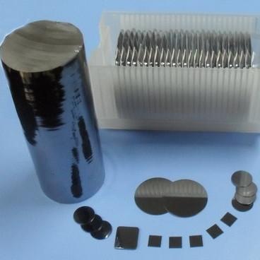
Si Crystal Substrate
Major Applications of Wafer Silicon
Wafer silicon is used in numerous hightechnology industries due to its versatility and exceptional material properties.
Semiconductor Device Manufacturing
Integrated circuits, processors, memory chips, analog devices, and microcontrollers are all fabricated on wafer silicon substrates through sophisticated lithography and deposition processes.
Power Electronics
Power MOSFETs, IGBTs, rectifiers, and highvoltage diodes rely on specialized wafer silicon designed for efficient power conversion and thermal management.
MEMS Devices
Microelectromechanical systems, including pressure sensors, accelerometers, gyroscopes, and microfluidic devices, are commonly manufactured using silicon wafers because of their excellent mechanical properties.
Photovoltaic Solar Cells
Monocrystalline wafer silicon remains one of the most widely used materials in highefficiency solar panels, converting sunlight into electricity with excellent longterm stability.
Optical and Photonic Components
Silicon wafers are increasingly used in silicon photonics for optical communication devices, waveguides, modulators, and integrated photonic circuits.
Research and Development
Universities, national laboratories, and research institutions use wafer silicon extensively for developing nextgeneration semiconductor technologies, quantum devices, nanoscale materials, and advanced sensors.
Advantages of Wafer Silicon
Wafer silicon continues to dominate semiconductor manufacturing because of its numerous technical and economic advantages.
Exceptional Material Quality
Ultrahigh purity and excellent crystal uniformity enable reliable production of highly integrated electronic devices with consistent performance.
Excellent Process Compatibility
Wafer silicon is compatible with virtually all major semiconductor fabrication technologies, including oxidation, ion implantation, chemical vapor deposition (CVD), physical vapor deposition (PVD), etching, and photolithography.
Outstanding Mechanical Strength
Silicon wafers maintain structural integrity throughout complex fabrication processes involving high temperatures and multiple chemical treatments.
Scalable Manufacturing
Available in multiple diameters and thicknesses, wafer silicon supports both laboratoryscale research and highvolume industrial production.
Cost Efficiency
Decades of manufacturing optimization have made silicon one of the most costeffective semiconductor materials available, offering an excellent balance between performance and affordability.
Broad Industry Acceptance
An extensive global supply chain, standardized specifications, and mature fabrication technologies make wafer silicon the preferred substrate for countless electronic applications.
Future Development Trends
As semiconductor technologies continue to evolve, wafer silicon is also advancing to meet increasingly demanding requirements. Larger wafer sizes, improved crystal quality, lower defect densities, and tighter dimensional tolerances are helping manufacturers achieve higher production yields and lower manufacturing costs.
In addition, innovations such as silicononinsulator (SOI) wafers, ultrathin wafers, epitaxial silicon wafers, and engineered substrates are expanding the capabilities of silicon for highfrequency communication, power electronics, artificial intelligence hardware, quantum computing, and advanced packaging technologies. These developments ensure that wafer silicon will remain a cornerstone material in the electronics industry for years to come.
Conclusion
Wafer silicon is the essential foundation upon which modern semiconductor technology is built. Its exceptional purity, outstanding crystal quality, superior thermal stability, and excellent electrical characteristics make it the preferred substrate for manufacturing integrated circuits, MEMS devices, power electronics, photovoltaic cells, and photonic components.
Through advanced manufacturing processes that include crystal growth, precision slicing, polishing, cleaning, and inspection, wafer silicon provides the reliability and consistency required for today's most sophisticated electronic products. As the demand for faster, smaller, and more energyefficient devices continues to increase, wafer silicon will remain an indispensable material driving innovation across the global semiconductor industry.


 Daisy@foam-material.com