item no :
Silicon-wafer/substrmoq :
1lead date :
In Stockpayment:
Credit Card L/C D/A D/P T/T Western Union
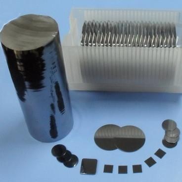
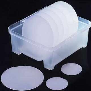
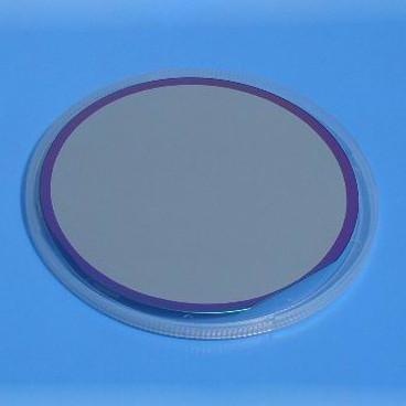
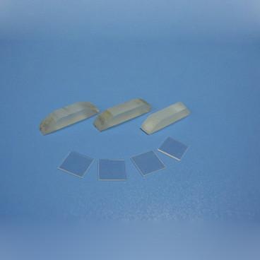
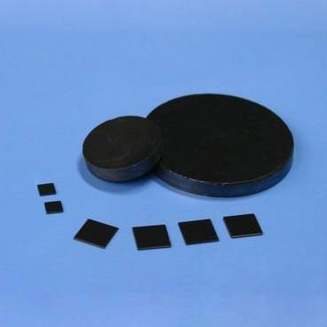
Silicon wafer for manufacturing semiconductor Silicon devices for high power rectifiers, high power transistors, diodes, switching devices, and the like. It is a promising material in the development of energy. The growth methods of single crystal Silicon include Czochralski method (CZ), Floating Zone method (FZ), and epitaxial method. The Czochralski Monocrystalline Silicon wafer is mainly used for a semiconductor integrated circuit, a diode, an epitaxial wafer substrate, and a solar cell.
|
The main performance parameter
|
|||
|
Crystal Structure
|
Cubic
|
||
|
Melting point(℃)
|
1420
|
||
|
Density
|
2.4(g/cm3)
|
||
|
Growth method
|
Float Zone (FZ)
Czochralski (CZ) magnetic field Czochralski method (MCZ) |
||
|
Dopant
|
Un-doped
|
Boron-doped
|
Phos-doped / As-doped
|
|
Conductivity Type
|
Intrinsic
|
P-type
|
N-type
|
|
Resistivity
|
>1000 Ω-cm
>10000 Ω-cm |
0.001~0.005 Ω-cm
0.01~0.09 Ω-cm 0.1~0.9 Ω-cm 1~10 Ω-cm 20~100 Ω-cm |
0.001~0.005 Ω-cm 0.01~0.09 Ω-cm 0.1~0.9 Ω-cm 1~10 Ω-cm 20~100 Ω-cm |
|
EPD
|
/
|
/
|
/
|
|
Oxygen Content(/cm3)
|
≤8x10¹⁷
|
≤8x10¹⁷
|
≤8x10¹⁷
|
|
Carbon Content(/cm3)
|
≤5x10¹⁶
|
≤5x10¹⁶
|
≤5x10¹⁶
|
|
Packing
|
Class-100 clean bag, class-1000 clean room
|
||
|
Special specification
|
We can customize Specific spcification upon requirements
|
||
| Standard Specification | |||||
| Product Name | Orientation | Standard Size | Thickness | Polishing | |
|
Silicon substrate/wafer (Un-doped or P-type or N-type) |
<100> ±0.5° <110> ±0.5° <111> ±0.5° <211> ±0.5° Or other off-angle |
10x10mm 10x5mm 5x5mm 20x20mm φ2" x 0.28mm φ3" x 0.38mm φ4" x 0.5mm φ6" x 0.625mm φ8" x 0.725mm φ12" x 0.775mm Or others |
0.1mm 0.2mm 0.28mm 0.38mm 0.5mm 0.525mm 0.625mm 1.0mm ±25μm Or others |
Fine ground Single side polished Double side polished Roughness: Ra<10A(1.0nm) Roughness: Ra<5A(0.5nm) |
Inquiry Online |

 Gallium oxide Ga2O3 single crystal substrate
Wechat:18832681205 Whatsapp :+86 18832681205 Email: Daisy@foam-material.com
 Thermal SiO2 oxide Silicon Wafer Crystal Substrate
Wechat:18832681205 Whatsapp :+86 18832681205 Email: Daisy@foam-material.com
 Gallium Nitride GaN Thin Film on Sapphire Wafer Single Crystal Substrate
Wechat:18832681205 Whatsapp :+86 18832681205 Email: Daisy@foam-material.com
 Gallium Nitride on Silicon Wafer Single Crystal Substrate
Wechat:18832681205 Whatsapp :+86 18832681205 Email: Daisy@foam-material.com
 Silicon On Insulator SOI wafer Single Crystal Substrate
Wechat:18832681205 Whatsapp :+86 18832681205 Email: Daisy@foam-material.com
 Bismuth Silicate Bi12SiO20 Wafer Single Crystal Substrate
Wechat:18832681205 Whatsapp :+86 18832681205 Email: Daisy@foam-material.com
 Lead Tungstate PbWO4 Wafer Single Crystal Substrate
Wechat:18832681205 Whatsapp :+86 18832681205 Email: Daisy@foam-material.com
 Calcium carbonate CaCO3 crystal substrate
Wechat:18832681205 Whatsapp :+86 18832681205 Email: Daisy@foam-material.com
 Lithium gallate LiGaO2 single crystal substrate
Wechat:18832681205 Whatsapp :+86 18832681205 Email: Daisy@foam-material.com
 Cadmium telluride Wafer CdTe Crystal Substrate
Wechat:18832681205 Whatsapp :+86 18832681205 Email: Daisy@foam-material.com
Copyright © Cheap Copper Foam, Iron Nickel Foam, Titanium Foam All Rights Reserved. Powered by dyyseo.com
the professional team to service !
 Daisy@foam-material.com