Xiamen Zopin New Material Limited Established in 2011, it is a new material industry with capabilities of independent research & development, production and sales as one. Our ISO9001:2012 factory covers an area of 6 hectares and a building area of 28,000 square meters, with annual production of high-performance metal foams of 250,000 square meters. Our R&D team is composed of academicians and experts from Tsinghua University, Polytechnic University of Hong Kong, Nanyang Technological University, and other domestic and foreign metal foam professionals. After many years’ endeavor, we now own our proprietary intellectual property rights in manufacturing high purity and high porosity metal foams.
SOI Wafer: Overview, Features, Manufacturing, Applications, Advantages, and Conclusion
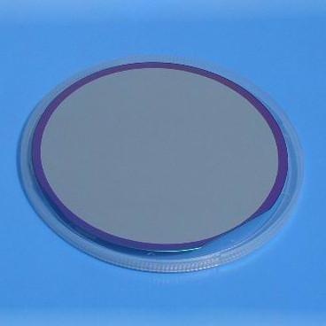
SOI wafer, or Silicon-On-Insulator wafer, is an advanced semiconductor substrate widely used in modern electronics and microelectromechanical systems (MEMS). An SOI wafer consists of a thin silicon layer separated from a bulk silicon substrate by a buried insulating layer, typically silicon dioxide. This structure significantly improves device performance, reduces parasitic capacitance, and enhances thermal and electrical characteristics, making SOI wafers indispensable in high-performance and low-power semiconductor applications.
Overview
SOI wafers are engineered to provide an insulating layer between the active silicon layer and the silicon substrate. This architecture reduces leakage currents, minimizes short-channel effects, and enhances switching speed in integrated circuits. SOI technology is particularly valuable for applications requiring high-frequency performance, low power consumption, and radiation hardness, such as in RF devices, automotive electronics, and aerospace applications. The choice of SOI wafer specifications, including thickness of the top silicon layer, buried oxide layer, and substrate type, directly impacts device performance and fabrication complexity.
Key Features of SOI Wafers
SOI wafers possess several distinctive features:
Reduced Parasitic Capacitance: Improves switching speed and lowers power consumption in transistors.
High-Performance Electrical Characteristics: Minimizes leakage currents and enhances device reliability.
Radiation Resistance: Enhanced tolerance to ionizing radiation, suitable for aerospace and defense electronics.
Thermal Isolation: Buried oxide layer provides thermal insulation, reducing self-heating in devices.
Thin and Uniform Top Silicon Layer: Allows precise device fabrication and scaling for advanced CMOS technology.
Compatibility with Standard CMOS Processes: SOI wafers can be integrated into existing semiconductor manufacturing workflows.
Manufacturing Process
The production of SOI wafers involves advanced techniques to achieve precise control over layer thickness, uniformity, and defect density:
SIMOX (Separation by IMplanted OXygen): Oxygen ions are implanted into a silicon wafer and thermally annealed to form a buried oxide layer.
Wafer Bonding (Smart Cut™): Two silicon wafers are bonded, one containing a thin silicon layer, and then a layer of silicon is split using hydrogen implantation to create the SOI structure.
Epitaxial Growth: A thin silicon layer is epitaxially grown on top of a buried oxide layer formed on a silicon substrate.
These processes allow precise control over the thickness of the top silicon layer, the buried oxide, and the substrate, which are critical for high-performance device fabrication.
Silicon-On-Insulator SOI wafer
Applications
SOI wafers are widely applied in high-performance and specialized semiconductor devices:
CMOS Technology: Low-power, high-speed transistors and integrated circuits for mobile, computing, and server applications.
RF and Microwave Devices: High-frequency amplifiers, switches, and components for telecommunications.
MEMS Devices: Sensors, actuators, and microfluidic devices benefit from electrical isolation and mechanical stability.
Power Electronics: Efficient power management devices with reduced leakage and enhanced thermal performance.
Automotive and Aerospace Electronics: Radiation-tolerant and high-reliability devices suitable for harsh environments.
Advantages
The main advantages of SOI wafers include:
Improved Device Performance: Higher switching speed, lower power consumption, and reduced short-channel effects.
Thermal and Electrical Isolation: Buried oxide layer reduces parasitic capacitance and thermal crosstalk.
Radiation Hardness: Enhanced reliability in space and defense applications.
Scalability: Supports aggressive scaling for next-generation semiconductor devices.
Compatibility: Integrates with standard CMOS processes for cost-effective manufacturing.
Durability: Reduced leakage currents and improved device lifespan.
Conclusion
In conclusion, SOI wafers are advanced semiconductor substrates offering superior electrical, thermal, and mechanical properties compared to conventional bulk silicon wafers. The unique layered structure, comprising a thin silicon layer over a buried oxide, enhances device performance, reduces power consumption, and provides radiation tolerance. SOI wafers are essential for modern high-performance, low-power, and specialized semiconductor applications, including CMOS devices, RF circuits, MEMS, and automotive electronics. With precise manufacturing techniques and excellent compatibility with standard fabrication processes, SOI wafers continue to drive innovation and reliability in the semiconductor industry.
 Daisy@foam-material.com