item no :
SOImoq :
1lead date :
In Stockpayment:
Credit Card L/C D/A D/P T/T Western Union
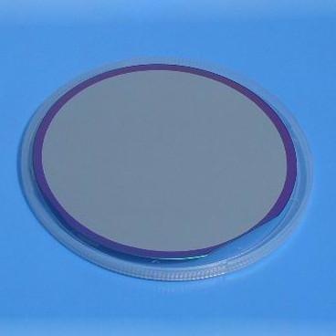
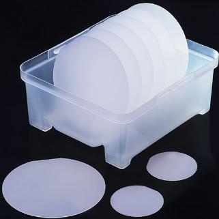
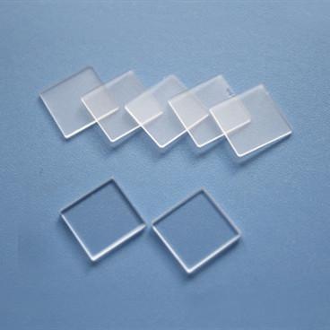
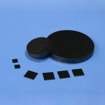
SOI wafer is mean the Silicon-On-Insulator wafer which is silicon on an insulating substrate (Si + SiO2 + Si), and a buried oxide layer is introduced between the top silicon and the back substrate.
By forming a semiconductor thin film on an insulator, SOI wafer materials have advantages that are incomparable to bulk silicon: It can realize the dielectric isolation of components in integrated circuits, completely eliminating the parasitic latch-up effect in bulk silicon CMOS circuits. The integrated circuit made of SOI also has the advantages of small parasitic capacitance, high integration density, high speed, simple process, smaller short channel effect, and especially suitable for low voltage and low power circuits. SOI will become the mainstream technology for deep submicron low voltage, low power integrated circuits. In addition, SOI materials are also used to fabricate MEMS optical switches,
|
Silicon-On-Insulator (SOI) wafer |
|
|
Structure |
Si + SiO2 + Si |
|
Standard Diameter |
4-inch(100mm), 6-inch(150mm), 8-inch(200mm) |
|
Orientation |
<100> |
|
Type/Dopant |
P-type/B-doped, N-type/P-doped |
|
Handle wafer thickness |
400um, 675um, 725um |
|
Resistivity |
1~20 ohm-cm, 1~100 ohm-cm, 0.001~0.005 ohm-cm or others |
|
|
|
|
Buried Oxide layer |
500nm, 1um, 2um, 3um |
|
|
|
|
Device layer |
70nm, 220nm, 340nm, 2um, 10um, 30um, 80um |
|
Orientation |
<100> |
|
Type/Dopant |
P-type/B-doped, N-type/P-doped, |
|
Resistivity |
1~20 ohm-cm, 1~100 ohm-cm, 0.001~0.005 ohm-cm or others |

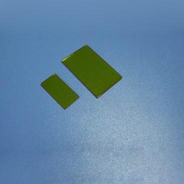
 Gallium oxide Ga2O3 single crystal substrate
Wechat:18832681205 Whatsapp :+86 18832681205 Email: Daisy@foam-material.com
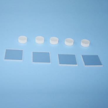
 Thermal SiO2 oxide Silicon Wafer Crystal Substrate
Wechat:18832681205 Whatsapp :+86 18832681205 Email: Daisy@foam-material.com
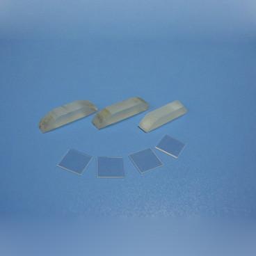
 Gallium Nitride GaN Thin Film on Sapphire Wafer Single Crystal Substrate
Wechat:18832681205 Whatsapp :+86 18832681205 Email: Daisy@foam-material.com
 Gallium Nitride on Silicon Wafer Single Crystal Substrate
Wechat:18832681205 Whatsapp :+86 18832681205 Email: Daisy@foam-material.com
 Bismuth Silicate Bi12SiO20 Wafer Single Crystal Substrate
Wechat:18832681205 Whatsapp :+86 18832681205 Email: Daisy@foam-material.com
 Lead Tungstate PbWO4 Wafer Single Crystal Substrate
Wechat:18832681205 Whatsapp :+86 18832681205 Email: Daisy@foam-material.com
 Calcium carbonate CaCO3 crystal substrate
Wechat:18832681205 Whatsapp :+86 18832681205 Email: Daisy@foam-material.com
 Lithium gallate LiGaO2 single crystal substrate
Wechat:18832681205 Whatsapp :+86 18832681205 Email: Daisy@foam-material.com
 Cadmium telluride Wafer CdTe Crystal Substrate
Wechat:18832681205 Whatsapp :+86 18832681205 Email: Daisy@foam-material.com
 Cadmium Sulfide Wafer CdS Single Crystal Substrate
Wechat:18832681205 Whatsapp :+86 18832681205 Email: Daisy@foam-material.com
Copyright © Cheap Copper Foam, Iron Nickel Foam, Titanium Foam All Rights Reserved. Powered by dyyseo.com
the professional team to service !
 Daisy@foam-material.com