item no :
Thermal-oxide-Silicomoq :
1lead date :
In Stockpayment:
Credit Card L/C D/A D/P T/T Western Union
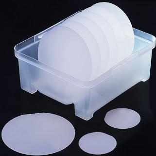
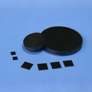
The Thermal oxide SiO2 layer is not only as a masking layer for ion implantation or thermal diffusion, and also a passivation layer that protects the surface of the device from the surrounding environment. It's not just an electrically isolated insulation between the device and another device. It is also a major component of MOS processes and electrical isolation in multilayer metallization systems.
|
Standard Specifications |
|
|
Product Name |
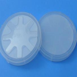
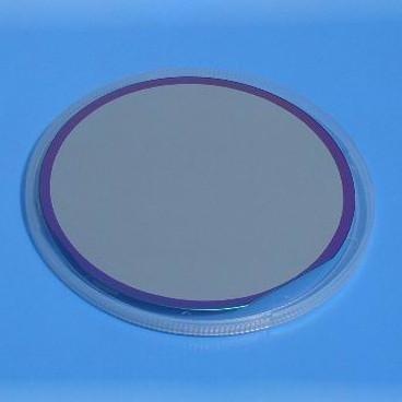
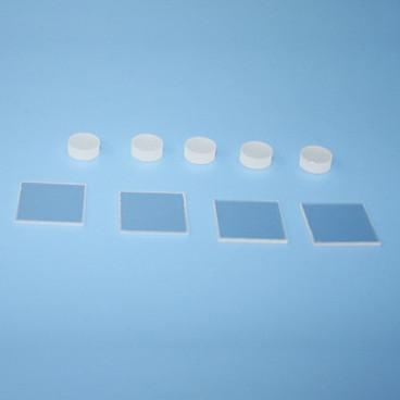
Thermal oxide Silicon wafer (SiO2/Si) |
|
|
|
|
Oxide-layer(SiO2 layer) |
25nm, 50nm, 100nm, 300nm, 500nm, 1um or others |
|
Oxidation surface |
Single-sided oxidation, Double-sided oxidation
|
|
Oxidation process |
Dry oxidation, Wet oxidation, |
|
|
|
|
Conductivity type/Dopant |
N-type/Phos-doped or N-type/As-doped or P-type/Boron-doped or Un-doped |
|
Orientation |
<100> or <111> |
|
Diameter of Silicon wafer |
2"(50.8mm), 3"(76.2mm), 4"(100mm), 6"(150mm), 8"(200mm), 12"(250mm) |
|
Thickness of Silicon wafer |
280um, 380um, 525um, 675um, 725um |
|
Resistivity (Ohm-cm) |
0.001~0.005, 0.01~0.09, 0.1~0.9, 1~10, 20~30, >100, >1000, >10000 |
|
Polishing |
Single side polished or Double side polished |
|
Surface Roughness |
Ra<5A (0.5nm) or Ra<10A (1.0nm) |

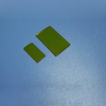
 Gallium oxide Ga2O3 single crystal substrate
Wechat:18832681205 Whatsapp :+86 18832681205 Email: Daisy@foam-material.com
 Gallium Nitride GaN Thin Film on Sapphire Wafer Single Crystal Substrate
Wechat:18832681205 Whatsapp :+86 18832681205 Email: Daisy@foam-material.com
 Gallium Nitride on Silicon Wafer Single Crystal Substrate
Wechat:18832681205 Whatsapp :+86 18832681205 Email: Daisy@foam-material.com
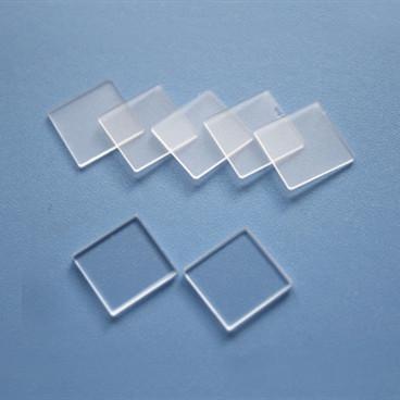
 Silicon On Insulator SOI wafer Single Crystal Substrate
Wechat:18832681205 Whatsapp :+86 18832681205 Email: Daisy@foam-material.com
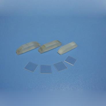
 Bismuth Silicate Bi12SiO20 Wafer Single Crystal Substrate
Wechat:18832681205 Whatsapp :+86 18832681205 Email: Daisy@foam-material.com
 Lead Tungstate PbWO4 Wafer Single Crystal Substrate
Wechat:18832681205 Whatsapp :+86 18832681205 Email: Daisy@foam-material.com
 Calcium carbonate CaCO3 crystal substrate
Wechat:18832681205 Whatsapp :+86 18832681205 Email: Daisy@foam-material.com
 Lithium gallate LiGaO2 single crystal substrate
Wechat:18832681205 Whatsapp :+86 18832681205 Email: Daisy@foam-material.com
 Cadmium telluride Wafer CdTe Crystal Substrate
Wechat:18832681205 Whatsapp :+86 18832681205 Email: Daisy@foam-material.com
 Cadmium Sulfide Wafer CdS Single Crystal Substrate
Wechat:18832681205 Whatsapp :+86 18832681205 Email: Daisy@foam-material.com
Copyright © Cheap Copper Foam, Iron Nickel Foam, Titanium Foam All Rights Reserved. Powered by dyyseo.com
the professional team to service !
 Daisy@foam-material.com