item no :
GaNmoq :
1lead date :
In Stockpayment:
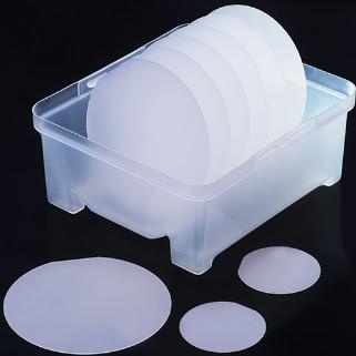
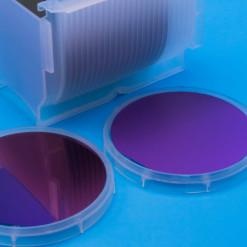
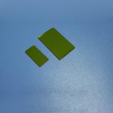
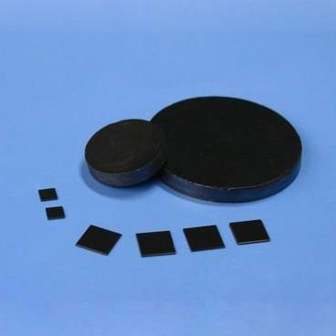
Credit Card L/C D/A D/P T/T Western UnionGallium Nitride GaN Thin Film on Sapphire Wafer Single Crystal Substrate
Sapphire is the most popular substrate material for GaN thin film growth. The advantages of GaN on Sapphire wafer are good chemical stability, no absorption of visible light, moderate price, and relatively mature manufacturing technology. But the thermal conductivity is relatively poor, suitable for use in the operation of low current devices.
|
Standard specifications |
|||
| Product Name: | GaN thin film on Sapphire wafer | ||
| Dopant and Conductivity: | N-type/Si-doped | N-type/Undoped | P-type/Mg-doped |
| Orientation: | C-plane, <0001> | ||
| Standard Size: |
Diameter 2"(50.8mm), Diameter 4"(100mm) |
||
| Standard Thickness: | 430um, 650um | ||
| GaN thin film: | 4.5um, 20um | 4.5um, 20um | 4.5um, 20um |
| Resistivity(300K): | <0.05 ohm-cm, | <0.5 ohm-cm | <10 ohm-cm |
| Carrier Concentration: | > 1x10E18 /cm3 | < 5x10E17 /cm3 | > 6x10E16 /cm3 |
| Mobility: | ~ 200 cm2/V•s | ~ 300 cm2/V•s | ~ 10 cm2/V•s |
| Dislocation density: | <5x10E8 cm-2 | <5x10E8 /cm2 | <5x10E8 cm-2 |
| Substrate | GaN on Sapphire substrate | GaN on Sapphire substrate | GaN on Sapphire substrate |
| Uable area: | >90% | >90% | >90% |
| Polishing | Standard: Single side polished, Option: Doulbe side polished | ||
| Packing |
Standard: each piece individual packed in one bag, class-100 clean bag, in class-1000 clean room |
||

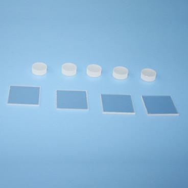
 Gallium oxide Ga2O3 single crystal substrate
Wechat:18832681205 Whatsapp :+86 18832681205 Email: Daisy@foam-material.com
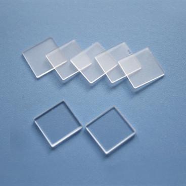
 Thermal SiO2 oxide Silicon Wafer Crystal Substrate
Wechat:18832681205 Whatsapp :+86 18832681205 Email: Daisy@foam-material.com
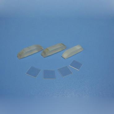
 Gallium Nitride on Silicon Wafer Single Crystal Substrate
Wechat:18832681205 Whatsapp :+86 18832681205 Email: Daisy@foam-material.com
 Silicon On Insulator SOI wafer Single Crystal Substrate
Wechat:18832681205 Whatsapp :+86 18832681205 Email: Daisy@foam-material.com
 Bismuth Silicate Bi12SiO20 Wafer Single Crystal Substrate
Wechat:18832681205 Whatsapp :+86 18832681205 Email: Daisy@foam-material.com
 Lead Tungstate PbWO4 Wafer Single Crystal Substrate
Wechat:18832681205 Whatsapp :+86 18832681205 Email: Daisy@foam-material.com
 Calcium carbonate CaCO3 crystal substrate
Wechat:18832681205 Whatsapp :+86 18832681205 Email: Daisy@foam-material.com
 Lithium gallate LiGaO2 single crystal substrate
Wechat:18832681205 Whatsapp :+86 18832681205 Email: Daisy@foam-material.com
 Cadmium telluride Wafer CdTe Crystal Substrate
Wechat:18832681205 Whatsapp :+86 18832681205 Email: Daisy@foam-material.com
 Cadmium Sulfide Wafer CdS Single Crystal Substrate
Wechat:18832681205 Whatsapp :+86 18832681205 Email: Daisy@foam-material.com
Copyright © Cheap Copper Foam, Iron Nickel Foam, Titanium Foam All Rights Reserved. Powered by dyyseo.com
the professional team to service !
 Daisy@foam-material.com