item no :
GaN2moq :
1lead date :
In Stockpayment:
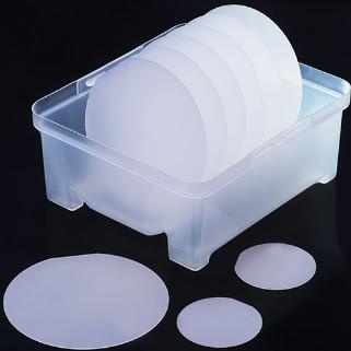
Credit Card L/C D/A D/P T/T Western UnionGallium Nitride on Silicon Wafer Single Crystal Substrate
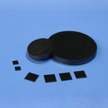
The GaN on Silicon wafer is to deposite a GaN thin film layer on semiconductor silicon wafer, by use this method to reduce costs and to replace Gallium Nitride single crystal substrate.
We can customize the GaN on Silicon wafer upon customer's requirements.
Standard Specification
ITEM
Gallium Nitride on Silicon wafer, GaN on Silicon wafer
GaN thin film
0.5μm ± 0.1 μm
GaN orientation
C-plane (0001)
Ga-face
<1nm, As-grown, EPI-ready
N-face
P-type/B-doped
Polarity
Ga-face
Conductivity type
Undoped/N-type
Macro defect density
Silicon wafer substrate
Orientation
<100>
Conductivity type
N-type/P-doped or P-type/B-doped
Dimension:
10 x 10 x 0.5mm, Single side polished
Resistivity
1-5 ohm-cm, 0-10 ohm-cm, <0.005 ohm-cm or others
<5/cm^2
Dia. 2” x 0.5mm, Single side polished
Dia. 4" x 0.525mm, Single side polished

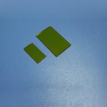
 Gallium oxide Ga2O3 single crystal substrate
Wechat:18832681205 Whatsapp :+86 18832681205 Email: Daisy@foam-material.com
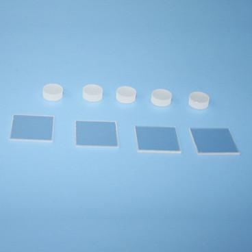
 Thermal SiO2 oxide Silicon Wafer Crystal Substrate
Wechat:18832681205 Whatsapp :+86 18832681205 Email: Daisy@foam-material.com
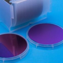
 Gallium Nitride GaN Thin Film on Sapphire Wafer Single Crystal Substrate
Wechat:18832681205 Whatsapp :+86 18832681205 Email: Daisy@foam-material.com
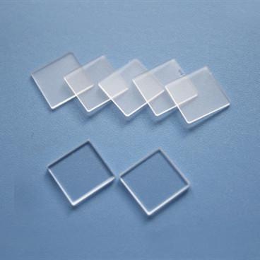
 Silicon On Insulator SOI wafer Single Crystal Substrate
Wechat:18832681205 Whatsapp :+86 18832681205 Email: Daisy@foam-material.com
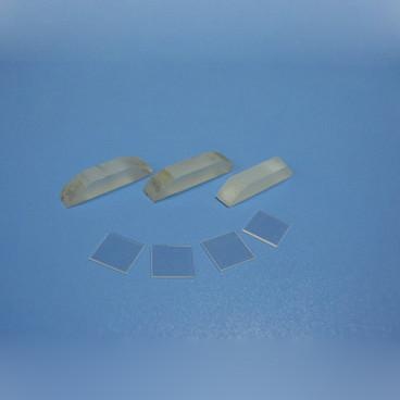
 Bismuth Silicate Bi12SiO20 Wafer Single Crystal Substrate
Wechat:18832681205 Whatsapp :+86 18832681205 Email: Daisy@foam-material.com
 Lead Tungstate PbWO4 Wafer Single Crystal Substrate
Wechat:18832681205 Whatsapp :+86 18832681205 Email: Daisy@foam-material.com
 Calcium carbonate CaCO3 crystal substrate
Wechat:18832681205 Whatsapp :+86 18832681205 Email: Daisy@foam-material.com
 Lithium gallate LiGaO2 single crystal substrate
Wechat:18832681205 Whatsapp :+86 18832681205 Email: Daisy@foam-material.com
 Cadmium telluride Wafer CdTe Crystal Substrate
Wechat:18832681205 Whatsapp :+86 18832681205 Email: Daisy@foam-material.com
 Cadmium Sulfide Wafer CdS Single Crystal Substrate
Wechat:18832681205 Whatsapp :+86 18832681205 Email: Daisy@foam-material.com
Copyright © Cheap Copper Foam, Iron Nickel Foam, Titanium Foam All Rights Reserved. Powered by dyyseo.com
the professional team to service !
 Daisy@foam-material.com