item no :
GaPmoq :
1lead date :
In Stockpayment:
Credit Card L/C D/A D/P T/T Western Union
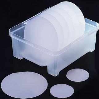
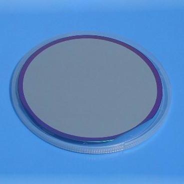
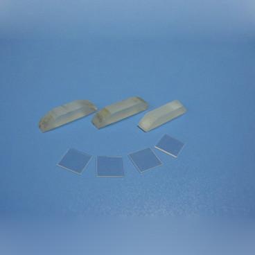
The crystal structure of Gallium Phosphide(GaP) is a sphalerite type, which is an indirect transition type semiconductor. It is one of the main substrate materials for LEDs.
The Gallium Phosphide(GaP) epitaxial material is obtained by liquid-phase epitaxy or vapor-phase epitaxy and diffusion growth on a gallium phosphide single crystal substrate. The GaP is mostly used to manufacture light-emitting diodes. The GaP liquid-phase epitaxial material can produce red, green, yellow-green light-emitting diodes. And the GaP Vapor-phase epitaxial and diffusion-grown material can produce yellow, yellow-green light-emitting diodes.
|
Substrate material |
Single crystal Gallium Phosphide (GaP) |
|
Crystal structure |
Cubic a =5.4505 Å |
|
Growth method |
Czochralski (CZ) |
|
Density: |
4.13 g/cm3 |
|
Melting point: |
1480 ℃ |
|
Coefficient of thermal expansion: |
5.3 x10⁻⁶ |
|
Doping: |
S-doped/N-type; Undoped/N-type |
|
Thermal conductivity: |
2~8 x10¹⁷/cm3; 4~ 6 x10¹⁶/cm3 |
|
Resistivity (W.cm) |
~0.03; ~0.3 |
|
EPD (cm-2 ): |
< 3x10E5; < 3x10E5 |
|
Standard Orientation |
<111> or <100> |
|
Standard size |
10x10x0.5mm, Dia2"x0.5mm, Dia2"x0.28mm |
|
Polishing |
Single side polished or Double side polished |

 Gallium oxide Ga2O3 single crystal substrate
Wechat:18832681205 Whatsapp :+86 18832681205 Email: Daisy@foam-material.com
 Thermal SiO2 oxide Silicon Wafer Crystal Substrate
Wechat:18832681205 Whatsapp :+86 18832681205 Email: Daisy@foam-material.com
 Gallium Nitride GaN Thin Film on Sapphire Wafer Single Crystal Substrate
Wechat:18832681205 Whatsapp :+86 18832681205 Email: Daisy@foam-material.com
 Gallium Nitride on Silicon Wafer Single Crystal Substrate
Wechat:18832681205 Whatsapp :+86 18832681205 Email: Daisy@foam-material.com
 Silicon On Insulator SOI wafer Single Crystal Substrate
Wechat:18832681205 Whatsapp :+86 18832681205 Email: Daisy@foam-material.com
 Bismuth Silicate Bi12SiO20 Wafer Single Crystal Substrate
Wechat:18832681205 Whatsapp :+86 18832681205 Email: Daisy@foam-material.com
 Lead Tungstate PbWO4 Wafer Single Crystal Substrate
Wechat:18832681205 Whatsapp :+86 18832681205 Email: Daisy@foam-material.com
 Calcium carbonate CaCO3 crystal substrate
Wechat:18832681205 Whatsapp :+86 18832681205 Email: Daisy@foam-material.com
 Lithium gallate LiGaO2 single crystal substrate
Wechat:18832681205 Whatsapp :+86 18832681205 Email: Daisy@foam-material.com
 Cadmium telluride Wafer CdTe Crystal Substrate
Wechat:18832681205 Whatsapp :+86 18832681205 Email: Daisy@foam-material.com
Copyright © Cheap Copper Foam, Iron Nickel Foam, Titanium Foam All Rights Reserved. Powered by dyyseo.com
the professional team to service !
 Daisy@foam-material.com