item no :
InAsmoq :
1lead date :
In Stockpayment:
Credit Card L/C D/A D/P T/T Western Union
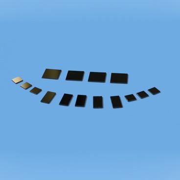
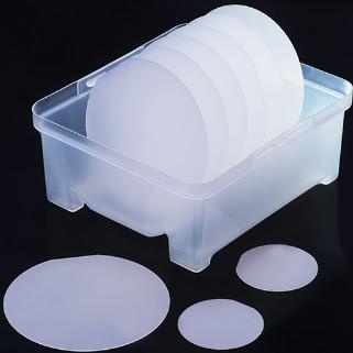
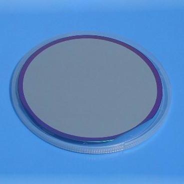
Indium arsenide, InAs substrate. InAs single crystal as a substrate can be use to grown InAsSb / In-AsPSb, InNAsSb and other heterojunction materials, Produced wavelength 2 ~ 14μm infrared light-emitting devices, InAs single crystal substrate can also be use to epitaxial growth a superlattice structure material AlGaSb, Produce mid-infrared quantum cascade laser.
|
The main performance parameters |
|||||||
|
Dopant
|
Conductivity type
|
Carrier Concentration
(cm-3) |
Mobility
(cm2/V.s) |
Dislocation density
(cm-2) |
Standard Size
|
||
|
InAs
|
Un-doped |
N-type
|
5 x 10¹⁶
|
2 x 10⁴
|
<5x10⁴
|
Φ2″x0.5mm
Φ3″x0.6mm
Φ4″x0.8mm |
|
|
InAs
|
Sn-doped
|
N-type
|
(5-20) x 1017
|
>2000
|
<5x10⁴
|
Φ2″x0.5mm
Φ3″x0.6mm
Φ4″x0.8mm |
|
|
InAs
|
Zn-doped
|
P-type
|
(1-20) x 1017
|
100-300
|
<5x10⁴
|
Φ2″x0.5mm
Φ3″x0.6mm
Φ4″x0.8mm |
|
|
InAs
|
S-doped
|
N-type
|
(1-10) x 1017
|
>2000
|
<5x10⁴
|
Φ2″x0.5mm
Φ3″x0.6mm
Φ4″x0.8mm |
|
| Orientation |
<100> / <111> ±0.5° Or other off-angle |
||||||
|
Standard Dimension
|
φ50.8x0.5mm, 10x10x0.5mm, 10x5x0.5mm
|
||||||
|
Surface roughness
|
(Ra):<=5A (0.5nm)
|
||||||
|
Polishing
|
Single side polished or Double side polished
|
||||||
| TTV / Bow / Warp |
2" wafer (TTV: <10 um, Bow: <10 um, Warp: <15 um) 3" wafer (TTV: <10 um, Bow: <10 um, Warp: <15 um) 4" wafer (TTV: <15 um, Bow: <15 um, Warp: <15 um) |
||||||
| Special specification | We can customize specific specification according to customer's requirements | ||||||

 Gallium oxide Ga2O3 single crystal substrate
Wechat:18832681205 Whatsapp :+86 18832681205 Email: Daisy@foam-material.com
 Thermal SiO2 oxide Silicon Wafer Crystal Substrate
Wechat:18832681205 Whatsapp :+86 18832681205 Email: Daisy@foam-material.com
 Gallium Nitride GaN Thin Film on Sapphire Wafer Single Crystal Substrate
Wechat:18832681205 Whatsapp :+86 18832681205 Email: Daisy@foam-material.com
 Gallium Nitride on Silicon Wafer Single Crystal Substrate
Wechat:18832681205 Whatsapp :+86 18832681205 Email: Daisy@foam-material.com
 Silicon On Insulator SOI wafer Single Crystal Substrate
Wechat:18832681205 Whatsapp :+86 18832681205 Email: Daisy@foam-material.com
 Bismuth Silicate Bi12SiO20 Wafer Single Crystal Substrate
Wechat:18832681205 Whatsapp :+86 18832681205 Email: Daisy@foam-material.com
 Lead Tungstate PbWO4 Wafer Single Crystal Substrate
Wechat:18832681205 Whatsapp :+86 18832681205 Email: Daisy@foam-material.com
 Calcium carbonate CaCO3 crystal substrate
Wechat:18832681205 Whatsapp :+86 18832681205 Email: Daisy@foam-material.com
 Lithium gallate LiGaO2 single crystal substrate
Wechat:18832681205 Whatsapp :+86 18832681205 Email: Daisy@foam-material.com
 Cadmium telluride Wafer CdTe Crystal Substrate
Wechat:18832681205 Whatsapp :+86 18832681205 Email: Daisy@foam-material.com
Copyright © Cheap Copper Foam, Iron Nickel Foam, Titanium Foam All Rights Reserved. Powered by dyyseo.com
the professional team to service !
 Daisy@foam-material.com