item no :
InPmoq :
1lead date :
In Stockpayment:
Credit Card L/C D/A D/P T/T Western Union
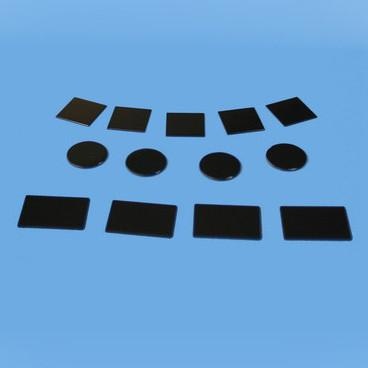
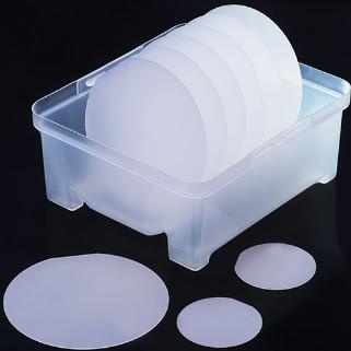
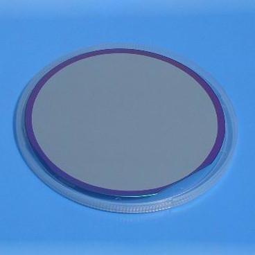
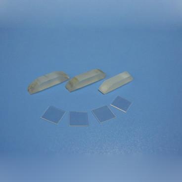
InP single crystal material is used as one of the most important compound semiconductor material, use to produce optical communications material of InP-based laser diode (LD), it is the key materials of Light emitting diode (LED) and photodetector, These devices realized message transmit , dissemination, amplification, reception and other functions in fiber-optic communications. InP is also very suitable for high frequency devices such as high electron mobility transistor (HEMT) and heterojunction bipolar transistor (HBT) and others.
Standard Specifications
Conductivity type
(cm2/V.s)
(cm-2)
Φ4"x0.6mm
Φ4"x0.6mm
Φ4"x0.6mm
Φ4"x0.6mm
φ50.8 x 0.35mm, φ76.2 x 0.5mm, φ100 x 0.6mm
We can customize Specific specification upon requirements

 Gallium oxide Ga2O3 single crystal substrate
Wechat:18832681205 Whatsapp :+86 18832681205 Email: Daisy@foam-material.com
 Thermal SiO2 oxide Silicon Wafer Crystal Substrate
Wechat:18832681205 Whatsapp :+86 18832681205 Email: Daisy@foam-material.com
 Gallium Nitride GaN Thin Film on Sapphire Wafer Single Crystal Substrate
Wechat:18832681205 Whatsapp :+86 18832681205 Email: Daisy@foam-material.com
 Gallium Nitride on Silicon Wafer Single Crystal Substrate
Wechat:18832681205 Whatsapp :+86 18832681205 Email: Daisy@foam-material.com
 Silicon On Insulator SOI wafer Single Crystal Substrate
Wechat:18832681205 Whatsapp :+86 18832681205 Email: Daisy@foam-material.com
 Bismuth Silicate Bi12SiO20 Wafer Single Crystal Substrate
Wechat:18832681205 Whatsapp :+86 18832681205 Email: Daisy@foam-material.com
 Lead Tungstate PbWO4 Wafer Single Crystal Substrate
Wechat:18832681205 Whatsapp :+86 18832681205 Email: Daisy@foam-material.com
 Calcium carbonate CaCO3 crystal substrate
Wechat:18832681205 Whatsapp :+86 18832681205 Email: Daisy@foam-material.com
 Lithium gallate LiGaO2 single crystal substrate
Wechat:18832681205 Whatsapp :+86 18832681205 Email: Daisy@foam-material.com
 Cadmium telluride Wafer CdTe Crystal Substrate
Wechat:18832681205 Whatsapp :+86 18832681205 Email: Daisy@foam-material.com
Copyright © Cheap Copper Foam, Iron Nickel Foam, Titanium Foam All Rights Reserved. Powered by dyyseo.com
the professional team to service !
 Daisy@foam-material.com