item no :
GaSbmoq :
1lead date :
In Stockpayment:
Credit Card L/C D/A D/P T/T Western Union
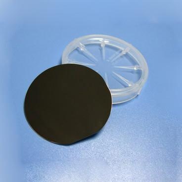
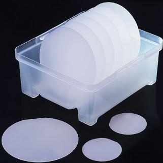
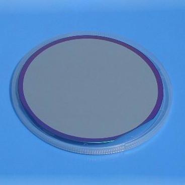
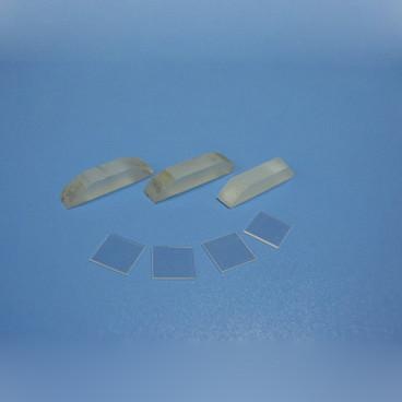
GaSb as a substrate material can be used for the production of certain infrared lasers and detectors of optical fiber transmission, GaSb is also foreseen with a lattice restriction mobility greater than GaAs, so that it has a potential application in the production of microwave devices. The main growth method GaS single crystal material, including traditional LEC Technology, improved LEC technology, Moving heating method / vertical gradient freeze technology (VGF) / vertical Bridgman technique (VBG) and other.
|
Standard Specifications |
|||||||
|
/
|
Dopant
|
Conductivity type
|
Carrier concentration
(cm-3)
|
Mobility
(cm2/V.s) |
Dislocation density
(cm-2) |
Standard size
|
|
|
GaSb
|
Undoped
|
P-type
|
(1~2) x 1017
|
600-700
|
《3000
|
Φ2"x0.5mm
Φ3"x0.6mm
Φ4"x0.8mm |
|
|
GaSb
|
Zn-doped
|
P-type
|
(5~100) x 1017
|
200-500
|
《3000
|
Φ2"x0.5mm
Φ3"x0.6mm
Φ4"x0.8mm |
|
|
GaSb
|
Te-doped
|
N-type
|
(1~20) x 1017
|
2000-3500
|
《3000
|
Φ2"x0.5mm
Φ3"x0.6mm
Φ4"x0.8mm |
|
| Orientation |
<100> / <111> ±0.5°
|
||||||
|
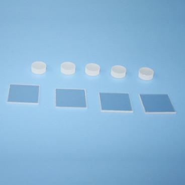
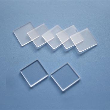
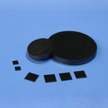
Standard dimension
|
20x20x0.5mm, 10x10x0.5mm, 10x5x0.5mm
Φ2"x0.5mm, Φ3"x0.6mm, Φ4"x0.8mm Or others upon customer's requirements |
||||||
|
Primary Orientation flat
Second Orientation flat |
16mm(Φ2"), 22mm(Φ3"), 32.5mm(Φ4") 8mm(Φ2"), 11mm(Φ3"), 16mm(Φ4") |
||||||
|
Surface roughness
|
Ra<=5A (0.5nm)
|
||||||
| Polishing |
Single side Polished or Double side polished
|
||||||
| TTV / Bow /Warp |
TTV <10um Bow <10um Warp <15um |
||||||
| Special specification | We can customize specific specification upon requirements | ||||||

 Gallium oxide Ga2O3 single crystal substrate
Wechat:18832681205 Whatsapp :+86 18832681205 Email: Daisy@foam-material.com
 Thermal SiO2 oxide Silicon Wafer Crystal Substrate
Wechat:18832681205 Whatsapp :+86 18832681205 Email: Daisy@foam-material.com
 Gallium Nitride GaN Thin Film on Sapphire Wafer Single Crystal Substrate
Wechat:18832681205 Whatsapp :+86 18832681205 Email: Daisy@foam-material.com
 Gallium Nitride on Silicon Wafer Single Crystal Substrate
Wechat:18832681205 Whatsapp :+86 18832681205 Email: Daisy@foam-material.com
 Silicon On Insulator SOI wafer Single Crystal Substrate
Wechat:18832681205 Whatsapp :+86 18832681205 Email: Daisy@foam-material.com
 Bismuth Silicate Bi12SiO20 Wafer Single Crystal Substrate
Wechat:18832681205 Whatsapp :+86 18832681205 Email: Daisy@foam-material.com
 Lead Tungstate PbWO4 Wafer Single Crystal Substrate
Wechat:18832681205 Whatsapp :+86 18832681205 Email: Daisy@foam-material.com
 Calcium carbonate CaCO3 crystal substrate
Wechat:18832681205 Whatsapp :+86 18832681205 Email: Daisy@foam-material.com
 Lithium gallate LiGaO2 single crystal substrate
Wechat:18832681205 Whatsapp :+86 18832681205 Email: Daisy@foam-material.com
 Cadmium telluride Wafer CdTe Crystal Substrate
Wechat:18832681205 Whatsapp :+86 18832681205 Email: Daisy@foam-material.com
Copyright © Cheap Copper Foam, Iron Nickel Foam, Titanium Foam All Rights Reserved. Powered by dyyseo.com
the professional team to service !
 Daisy@foam-material.com