item no :
GaNmoq :
1lead date :
In Stockpayment:
Credit Card L/C D/A D/P T/T Western Union
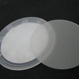
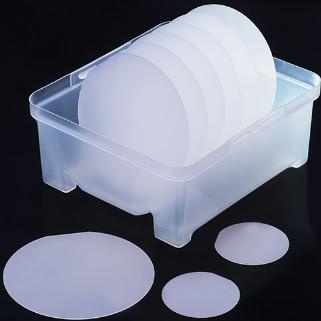
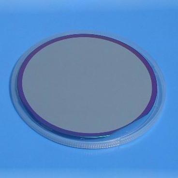
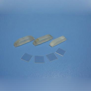
Gallium nitride, GaN substrate. GaN has a wide direct bandgap, strong atomic bonds and high thermal conductivity, etc., and it is a strong ability on anti-radiation, Not only is the short-wavelength optoelectronic materials, Also the replacement materials of high temperature semiconductor device, GaN can be used to make blue and green LED, or violet, ultraviolet light LD, ultraviolet detectors and high-frequency high-power electronic devices.
| GaN single crystal substrate/wafer | ||||
| Grade | S-level | A-level | B-level | C-level |
| Standard Size | 5X5.5mm, 10x10.5mm, 14x15mm, φ50.8mm, φ100mm | |||
| Standard Thickness | 350 ± 20 μm; 500 ± 20 μm | |||
| Marco Defect Density | <0 /cm2 | <0.3 /cm2 | <1 /cm2 | <4 /cm2 |
| Orientation | C-plane <0001> ± 0.5º | |||
|
Primary Orientation flat Second Orientation flat |
<1-100> ± 0.5°, 16mm(2-inch) / 30mm(4-inch)
<11-20> ± 3°, 8mm(2-inch) / 15mm(4-inch)
|
|||
| TTV | <= 15 μm | |||
| BOW | <= 20 μm | |||
| Dopant / Conductive |
Undoped/N-type (Resistivity: < 0.5 Ω-cm) Semi-insulating/Fe-doped (Resistivity: > 10E6 Ω-cm) Si-doped/N-type (Resistivity: < 0.05 Ω-cm ) |
|||
| Dislocation Density | <3x106 cm-2 | <3x106 cm-2 | <3x106 cm-2 | |
| Useable surface area | >90% | >80% | >70% | |
| Max size of macro defects | < 700 μm | < 2000 μm | < 4000 μm | |
| Polishing |
Ga-face surface roughness: Ra <0.3nm (Epitaxy-ready) N-face surface roughness: Ra 0.5 ~1.5 μm (optional: Ra <0.3 nm (polished)) |
|||
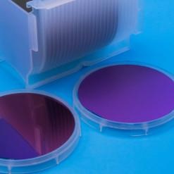
| Packing | Each piece individual packed in one bag, with class-100 clean bag | |||

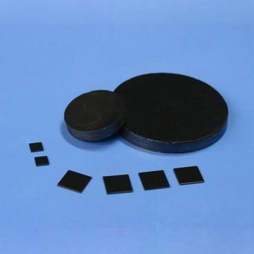
 Gallium oxide Ga2O3 single crystal substrate
Wechat:18832681205 Whatsapp :+86 18832681205 Email: Daisy@foam-material.com
 Thermal SiO2 oxide Silicon Wafer Crystal Substrate
Wechat:18832681205 Whatsapp :+86 18832681205 Email: Daisy@foam-material.com
 Gallium Nitride GaN Thin Film on Sapphire Wafer Single Crystal Substrate
Wechat:18832681205 Whatsapp :+86 18832681205 Email: Daisy@foam-material.com
 Gallium Nitride on Silicon Wafer Single Crystal Substrate
Wechat:18832681205 Whatsapp :+86 18832681205 Email: Daisy@foam-material.com
 Silicon On Insulator SOI wafer Single Crystal Substrate
Wechat:18832681205 Whatsapp :+86 18832681205 Email: Daisy@foam-material.com
 Bismuth Silicate Bi12SiO20 Wafer Single Crystal Substrate
Wechat:18832681205 Whatsapp :+86 18832681205 Email: Daisy@foam-material.com
 Lead Tungstate PbWO4 Wafer Single Crystal Substrate
Wechat:18832681205 Whatsapp :+86 18832681205 Email: Daisy@foam-material.com
 Calcium carbonate CaCO3 crystal substrate
Wechat:18832681205 Whatsapp :+86 18832681205 Email: Daisy@foam-material.com
 Lithium gallate LiGaO2 single crystal substrate
Wechat:18832681205 Whatsapp :+86 18832681205 Email: Daisy@foam-material.com
 Cadmium telluride Wafer CdTe Crystal Substrate
Wechat:18832681205 Whatsapp :+86 18832681205 Email: Daisy@foam-material.com
Copyright © Cheap Copper Foam, Iron Nickel Foam, Titanium Foam All Rights Reserved. Powered by dyyseo.com
the professional team to service !
 Daisy@foam-material.com